Byu Clean Room

Welcome To The Byu Cleanroom The Integrated Microfabrication Lab Byu Cleanroom

Cleanroom

Map Byu Cleanroom

Bruce Fernace

Access The Cleanroom

Byu New Heritage How Will I Fix This Up Hmm Pinterest College Dorm Decorations Hall Room College Living

Feedback bug reporting.
Byu clean room.

Laurell Spinner Byu Cleanroom

Byu Dorms Dorm Room Inspiration Girls Dorm Room Dorm Room Hacks
Byu Equipment Staff Embraces Moving Targets To Keep Football Team Safe During Pandemic Ksl Sports

Laser Mask Writer Byu Cleanroom

Su 8 3000 Datasheet From Microchem Byu Cleanroom

Harold Gets Hotter Byu Magazine

It S All In The Details Hinckley Hall Byu In 2020 College Dorm Room Decor Dorm Room Decor College Room

Diy Boys Room Reveal Ut Vs Byu Boys Room Diy Rooms Reveal Boy S Room

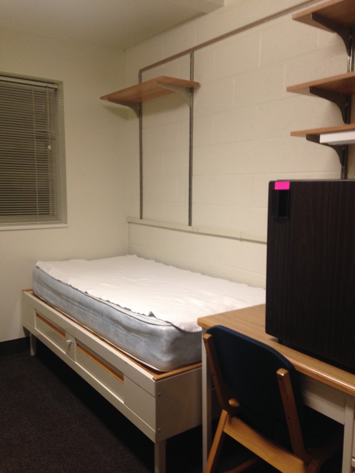
Byu On Campus Housing House Byu Room

Byu Painted Wall Google Search Man Cave Decor Sports Room Hunter Room

Byu Football Room Byu Football Brigham Young University Byu

Homemade Air Cleaner Byu Style Shop Dust Collection Air Filtration System Dust Collection System

It S All In The Details Hinckley Hall Byu College Dorm Room Decor Dorm Room Inspiration College Dorm Essentials

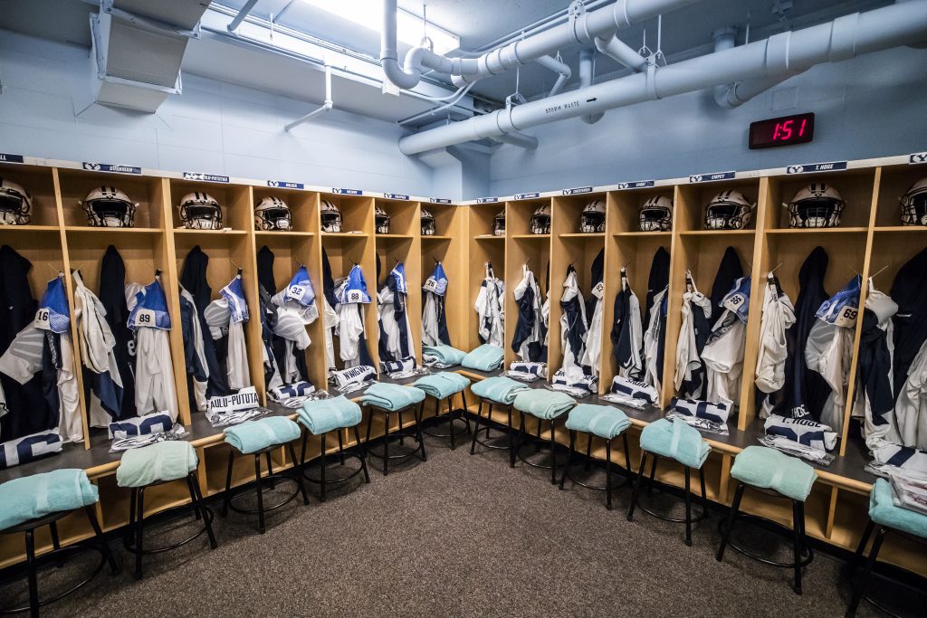
Volleyball Facilities The Official Site Of Byu Athletics Byu Byu Utah Byu Football

Diy Boys Room Reveal Ut Vs Byu Boys Room Diy Diy Boy Bedroom Rooms Reveal
It S All In The Details David John Hall Byu

Byu Wall Byu Mancave Byu Man Cave Byu Cougars Byu Football Room Room Ideas Bedroom Man Room Boy Wall Art
Football Facilities The Official Site Of Byu Athletics Byu Football Byu Football
Https Encrypted Tbn0 Gstatic Com Images Q Tbn 3aand9gcrcokiklsq1w5agsletmdy8yfm0fwsi6t O1edusaoeyvhccdj Usqp Cau

A Byu Blog Spectacular Byu Dorm Room Hacks Dorm Room Hacks Cool Dorm Rooms Dorm Room Diy
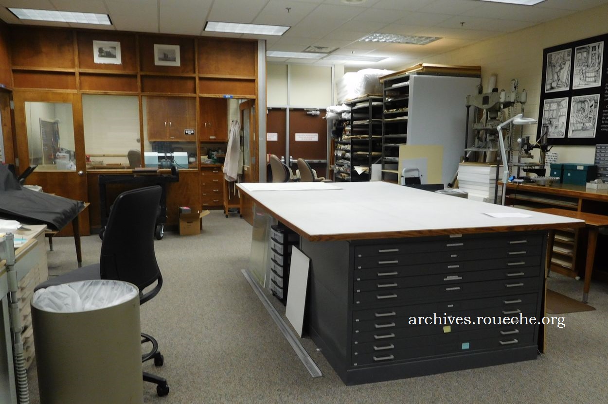
Field Trip Byu Book Conservation Lab Archiventures

Apartment For Rent At 915 N 150 E Provo Ut 84604 Rentler

A Freshman S Guide To Packing For Heritage Halls Modern Bathroom Decor Bathroom Decor Apartment Cool Dorm Rooms
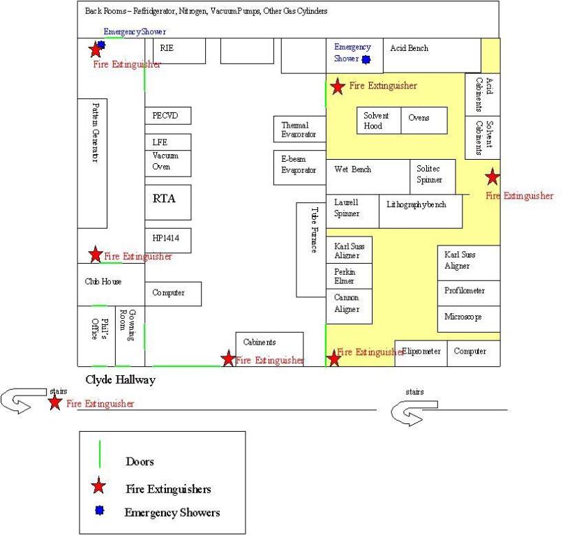
Fire Safety
Source : pinterest.com
